

Maximum Continuous Drain Current: 160 A
Width: 6.22mm
Transistor Configuration: Single
Maximum Drain Source Voltage: 40 V
Maximum Gate Threshold Voltage: 4V
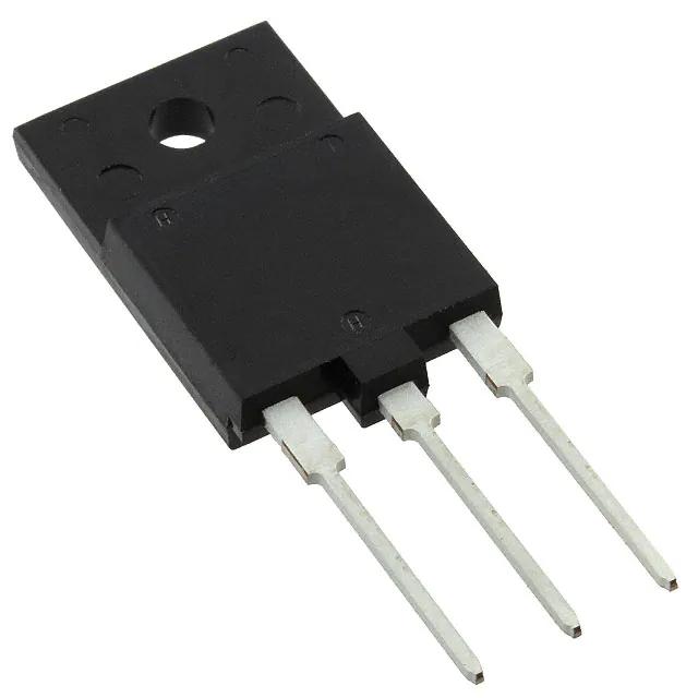
Package Type: DPAK
Number of Elements per Chip: 1
Minimum Gate Threshold Voltage: 2V
Maximum Operating Temperature: +175 °C
Typical Gate Charge @ Vgs: 80.6 nC @ 10 V
Channel Type: N
Length: 6.73mm
Pin Count: 3 Channel Mode: Enhancement Mounting Type: Surface Mount Maximum Power Dissipation: 120 W Maximum Gate Source Voltage: ±20 V Height: 2.25mm Minimum Operating Temperature: -55 °C Forward Diode Voltage: 1.2V Maximum Drain Source Resistance: 2.1 mΩ Base Part Number: NTD5C434 Detailed Description: N-Channel 40V 33A (Ta), 160A (Tc) 4.7W (Ta), 120W (Tc) Surface Mount DPAK Input Capacitance (Ciss) (Max) @ Vds: 5400pF @ 25V Drive Voltage (Max Rds On, Min Rds On): 10V Mounting Type: Surface Mount Vgs(th) (Max) @ Id: 4V @ 250µA Drain to Source Voltage (Vdss): 40V Vgs (Max): ±20V Gate Charge (Qg) (Max) @ Vgs: 80.6nC @ 10V Rds On (Max) @ Id, Vgs: 2.1mOhm @ 50A, 10V Supplier Device Package: DPAK Packaging: Cut Tape (CT) Operating Temperature: -55°C ~ 175°C (TJ) FET Type: N-Channel Customer Reference: Package / Case: TO-252-3, DPak (2 Leads + Tab), SC-63 Power Dissipation (Max): 4.7W (Ta), 120W (Tc) Current – Continuous Drain (Id) @ 25°C: 33A (Ta), 160A (Tc) Technology: MOSFET (Metal Oxide) Manufacturer: ON Semiconductor
This ismanufactured by ON Semiconductor. The manufacturer part number is NTD5C434NT4G. While 160 a of maximum continuous drain current. Furthermore, the product is 6.22mm wide. The product offers single transistor configuration. It has a maximum of 40 v drain source voltage. The product carries 4v of maximum gate threshold voltage. The package is a sort of dpak. It consists of 1 elements per chip. Whereas its minimum gate threshold voltage includes 2v. It has a maximum operating temperature of +175 °c. With a typical gate charge at Vgs includes 80.6 nc @ 10 v. The product is available in [Cannel Type] channel. Its accurate length is 6.73mm. It contains 3 pins. The product carries enhancement channel mode. The product is available in surface mount configuration. Provides up to 120 w maximum power dissipation. It features a maximum gate source voltage of ±20 v. In addition, the height is 2.25mm. Whereas, the minimum operating temperature of the product is -55 °c. Its forward diode voltage is 1.2v . It provides up to 2.1 mω maximum drain source resistance. Base Part Number: ntd5c434. It features n-channel 40v 33a (ta), 160a (tc) 4.7w (ta), 120w (tc) surface mount dpak. The product’s input capacitance at maximum includes 5400pf @ 25v. The drive voltage (maximum and minimum Rds On) of the product includes 10v. The typical Vgs (th) (max) of the product is 4v @ 250µa. The product has a 40v drain to source voltage. The maximum Vgs rate is ±20v. The maximum gate charge and given voltages include 80.6nc @ 10v. It has a maximum Rds On and voltage of 2.1mohm @ 50a, 10v. dpak is the supplier device package value. In addition, cut tape (ct) is the available packaging type of the product. The product has -55°c ~ 175°c (tj) operating temperature range. It carries FET type n-channel. Moreover, the product comes in to-252-3, dpak (2 leads + tab), sc-63. The product carries maximum power dissipation 4.7w (ta), 120w (tc). The continuous current drain at 25°C is 33a (ta), 160a (tc). This product use mosfet (metal oxide) technology. The on semiconductor’s product offers user-desired applications.

Reviews
There are no reviews yet.