

Maximum Continuous Drain Current: 120 A
Transistor Material: Si
Width: 9.25mm
Transistor Configuration: Single
Maximum Drain Source Voltage: 60 V
Maximum Gate Threshold Voltage: 4V
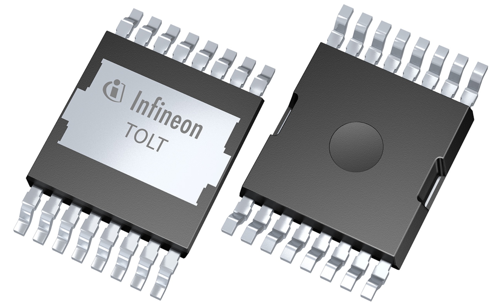
Package Type: D2PAK (TO-263)
Number of Elements per Chip: 1
Minimum Gate Threshold Voltage: 2V
Maximum Operating Temperature: +175 °C
Typical Gate Charge @ Vgs: 150 nC @ 10 V
Channel Type: N
Length: 10mm Pin Count: 3 Channel Mode: Enhancement Mounting Type: Surface Mount Maximum Power Dissipation: 188 W Series: OptiMOS™ -T2 Maximum Gate Source Voltage: -20 V, +20 V Height: 4.4mm Minimum Operating Temperature: -55 °C Maximum Drain Source Resistance: 2.8 mΩ
This is N-channel MOSFET 120 A 60 V OptiMOS T2 3-Pin D2PAK manufactured by Infineon. The manufacturer part number is IPB120N06S402ATMA2. While 120 a of maximum continuous drain current. The transistor is manufactured from highly durable si material. Furthermore, the product is 9.25mm wide. The product offers single transistor configuration. It has a maximum of 60 v drain source voltage. The product carries 4v of maximum gate threshold voltage. The package is a sort of d2pak (to-263). It consists of 1 elements per chip. Whereas its minimum gate threshold voltage includes 2v. It has a maximum operating temperature of +175 °c. With a typical gate charge at Vgs includes 150 nc @ 10 v. The product is available in [Cannel Type] channel. Its accurate length is 10mm. It contains 3 pins. The product carries enhancement channel mode. The product is available in surface mount configuration. Provides up to 188 w maximum power dissipation. The product optimos™ -t2, is a highly preferred choice for users. It features a maximum gate source voltage of -20 v, +20 v. In addition, the height is 4.4mm. Whereas, the minimum operating temperature of the product is -55 °c. It provides up to 2.8 mω maximum drain source resistance.
Reviews
There are no reviews yet.